Laser Direct Structuring (LDS) / Moulded Interconnect Devices (MID) for custom Antennas and unique Electromechanical solutions


DMTL are now able to offer limitless possibilities of Antenna design and support with the Ethertronics offering of Laser Direct Structuring (LDS)
For many years electronic products have often been governed by the size and shape of the PCB(s) within the assembly and this is often based on the number and complexity of the circuits. With the advent of multilayer flexible PCB’s and component miniaturisation, modern electronic products are now vastly different to that of products in the past. Engineers now have access to Rigid, Flexi-rigid and fully Flexible PCB’s to integrate into their designs which has allowed them the freedom to come up with mechanical designs which were once impossible to produce.
The consumer electronics industry has been at the forefront of pushing mechanical design limits in miniaturisation and appealing industrial design. Whilst a modern smart phone already utilises modern PCB techniques, such as having a mixture of Rigid and Flexible PCB’s they have also been using another technology for a number of years – Laser Direct Structuring (LDS). LDS is a process where a laser is used to expose conductive structures within an injection-moulded plastic part. The exposed trace(s) can then be metallised using a plating process to allow for connection within an electromechanical assembly.
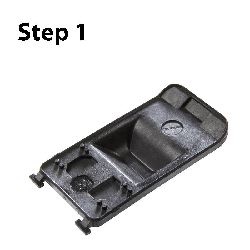
LDS in more detail - The process
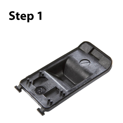
1) Injection Moulding
LDS suitable resin are loaded with additives and moulded to the desired shapes with traditional moulding tools. The part can be complex 3D shape with no real limitations.
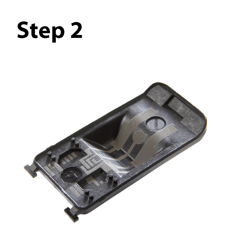
2) Laser Activation and Structuring
A special laser is used to trace the circuit design onto the plastic part. The laser creates a physical-chemical reaction, altering the parts surface and produces metallic nuclei – this is the activation process. In addition to the activation, the laser forms a microrough surface on which copper firmly anchors itself during metallisation.
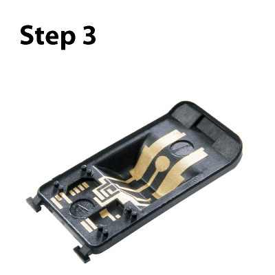
3) Metallisation
The parts conductive traces are built up during electroless copper baths. Finally, an electroless application of nickel and a thin gold layer is carried out to provide the best conductive finish.
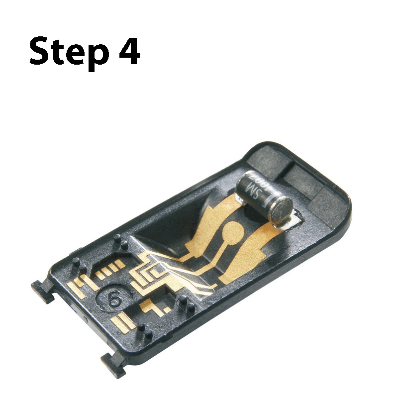
4) Assembly
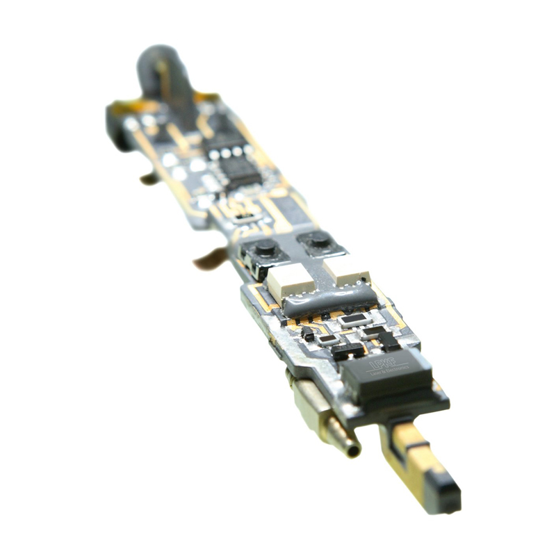
If component parts are to be attached directly onto the device, they can be placed with a standard SMT process.
5) Optional Finishing
If the part is cosmetic, various finishes can be applied to part to insulate and hide any of the conductive traces.
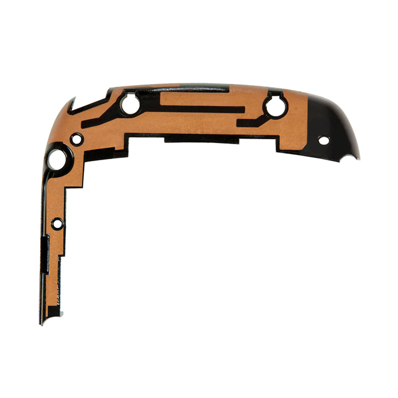
LDS Antennas
In today’s connected world, most new electronics come to the market with some sort of wireless connectivity. Whether it’s Bluetooth, Wifi, Cellular (3G, 4G, LTE), GPS or SATCOM integrating the correct Antenna into the product is not a trivial process and should therefore not be an afterthought. With this in mind it’s clear that the selection of the Antenna should be an early and critical design consideration to provide the very best signal strength and peak performance to the end product. LDS allows for the Antenna design to be created on the outside of the device and then simply connected into the circuit at a suitable location. This can therefore aid in wireless performance and the overall mechanical design of the product. Finishing processes following on from LDS Antenna production can leave the Antenna indistinguishable to the human eye which allows for modern industrial design.
What else can this technology be used for?
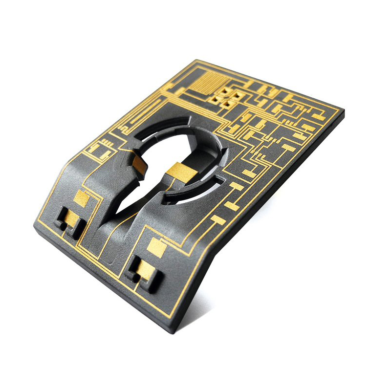
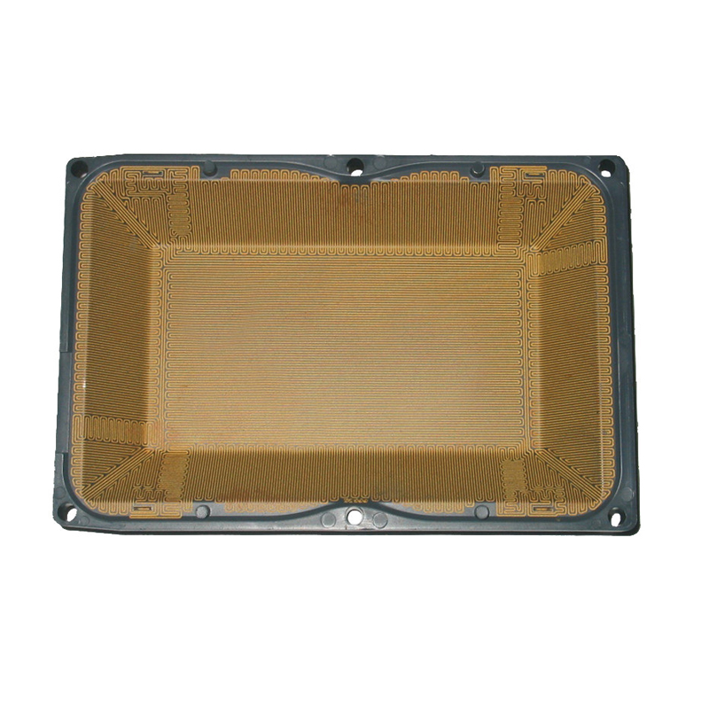
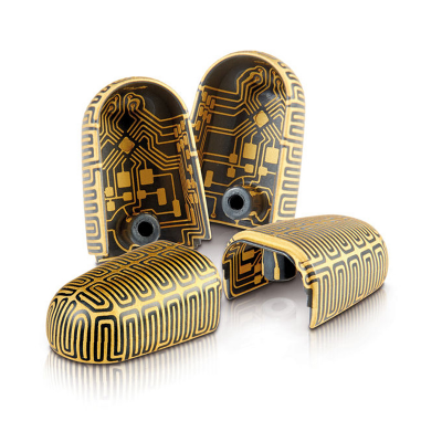
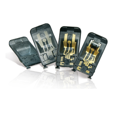
Whilst the most common use of LDS is to create Antennas, the technology can also be used to create Moulded Interconnect Devices (MID) – This provides almost limitless possibilities for product design – Effectively creating 3D PCB’s. Moulded Interconnect Devices allow for simple parts to be placed and soldered directly onto the plastic assembly with traditional pick and place processes. Furthermore, soldering techniques such a reflow and vapour phase can be used to mount components when specific heat resistance plastic blends are used. Parts can also be produced with reliable Through-hole plating to further expand the possibilities of design and layout.
Examples of Moulded Interconnect Devices
- Medical Devices
- High Security (Tamper Protection)
- Automotive Electronics
- Point of Sale
- Consumer Electronics
- Electronics Packaging
- Connectors
- Switches